
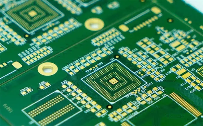
A compact circuit board can become difficult to route long before it runs out of space for components. Fine-pitch ball grid arrays (BGAs) need escape routes, power connections compete with signal traces, and conventional through-hole vias occupy valuable routing channels. Adding more layers may help, but it does not always solve the bottleneck beneath a dense package.
High-density interconnect (HDI) technology gives designers smaller interconnects and more control over which layers those connections reach. This HDI PCB guide explains when that flexibility is useful, how to choose a practical construction, and what to confirm before sending a design into production.
What Is an HDI PCB?
An HDI PCB is a printed circuit board that achieves higher interconnection density through features such as microvias, fine traces and spaces, and compact capture pads. Many designs also use blind vias, buried vias, and via-in-pad routing to connect densely packed components.
The distinction is the interconnect architecture. A conventional plated through-hole crosses the entire board, taking up space on layers where no connection is needed. A blind microvia can connect an outer layer to the adjacent inner layer while leaving deeper routing layers available.
HDI is common in smartphones, wearables, compact embedded systems, and other products with demanding package or enclosure constraints. It can also support high-speed designs by enabling shorter connections and smaller via stubs. Those benefits depend on the layout, materials, and return paths; the HDI label alone does not guarantee better electrical performance.
HDI PCB vs. Conventional Multilayer PCB
HDI does not require every connection to be a microvia. Through-holes can remain useful for connectors, power distribution, or connections across multiple layers. A practical design uses each via type where it solves a specific problem.
Decide Whether Your Board Needs HDI
Start with the component that is hardest to escape, usually a dense BGA or chip-scale package. Examine its ball pitch, pad dimensions, populated ball pattern, signal count, and power and ground assignments. Pitch alone cannot determine whether HDI is necessary.
Build a representative fan-out using the fabricator's production design rules. Check how many signals can leave the package on each layer, whether power connections remain practical, and whether critical signals retain suitable reference planes.
If conventional vias can route the design within the required size and layer count, compare that option with HDI before committing. If via pads block the escape channels or the enclosure cannot accommodate a larger board, microvias may address the actual constraint.
For example, a small wireless module may need HDI mainly to escape its processor package. An industrial controller with generous board area may route successfully with conventional multilayer construction. Both decisions should follow the routing study and operating requirements.
Understand the Via Options Before Choosing a Stackup
Four terms describe different aspects of an interconnect:
-
Through-hole via: passes through the full board thickness.
-
Blind via: connects an outer layer to one or more inner layers without passing through the full board.
-
Buried via: connects internal layers and is enclosed within the finished board.
-
Microvia: a small, shallow interconnect, commonly laser drilled in HDI buildup layers.
These categories overlap. A microvia can be blind, or it can become buried after additional layers are laminated above it.
Microvias can also be staggered or stacked. Staggered microvias are offset from one another and connected through an intermediate conductor. Stacked microvias sit directly above one another, creating a compact vertical connection. Stacking can save routing area, but the interfaces between the vias require careful process control and qualification.
Via-in-pad describes the location of a via within a component's solder pad. It can simplify BGA escape routing and shorten connections. The filling, planarization, and copper-cap requirements must suit the via construction and assembly process. Leaving an unsuitable open via in a solder pad can draw solder away from the joint.
Choose the Simplest Stackup That Routes Successfully
Common HDI constructions use notation such as 1+N+1 and 2+N+2. Here, N represents the copper layers in the central subassembly, while the outside numbers identify buildup layers on each side. A 1+4+1 construction therefore has six copper layers in total.
A 1+N+1 stackup provides one buildup layer on each side. It is a useful starting point when a single microvia level can release the outer-layer routing bottleneck. A 2+N+2 construction provides additional buildup layers and more interconnect options, with added processing and registration demands.
Any-layer HDI, often called every-layer interconnect, allows more flexible connections throughout the stack. It can support exceptionally dense layouts, but its manufacturing demands should be justified by the routing requirement.
Confirm the actual layer connections rather than relying on a stackup name. Two boards with the same total layer count can have different via structures, process sequences, costs, and reliability considerations.
The initial stackup review should establish signal and plane assignments, dielectric thicknesses, material choices, finished board thickness, and permitted via spans. It should also define impedance requirements and copper balance. Complete this review before detailed routing, when changes are still manageable.
Set Design Rules Around the Production Process
The smallest feature advertised on a capability sheet may represent a special process rather than the factory's preferred production geometry. Ask for rules appropriate to your materials, copper thickness, construction, and expected volume.
Microvia aspect ratio deserves particular attention. It compares via depth with diameter, and a deeper hole at the same diameter can become harder to metallize and fill reliably. Confirm how the fabricator defines and measures that diameter, especially for tapered laser-drilled holes.
Also obtain the required capture-pad dimensions, registration allowances, trace-to-pad clearances, and spacing between microvias. A nominal hole size is only one part of the geometry needed to manufacture a reliable connection.
For high-speed nets, agree on impedance targets and tolerances using the proposed stackup. Narrow traces and thin dielectrics affect impedance, losses, and fabrication tolerances. Provide continuous reference planes where needed and suitable return-path connections when signals change layers.
Power and thermal design need their own checks. A small microvia's current capacity depends on its geometry and copper construction. Dense routing does not replace current-capacity calculations, thermal analysis, or adequate copper paths for heat removal.
How HDI PCBs Are Manufactured
The exact process varies by construction, but a common sequence starts with imaging, etching, drilling, and plating the central subassembly. The factory then laminates buildup dielectric and copper, creates microvias, cleans and prepares the holes, and deposits copper to form the connections. Filling and planarization are added where required.
Further buildup stages repeat selected operations until the layer structure is complete. Outer-layer processing, solder mask, surface finishing, profiling, and inspection follow according to the approved manufacturing route.
Each additional stage introduces process time and another opportunity for registration, filling, or material problems. This explains why two boards with identical dimensions and layer counts can have substantially different quotes.
When evaluating an HDI PCB Manufacturer, ask for a review of your proposed stackup and via map. Confirm which features use routine production processes, which require special handling, and what inspection or qualification evidence will accompany the build.
Treat Microvia Reliability as a Design Requirement
An electrical test confirms connectivity at the time of testing. It does not establish that every interconnect will survive assembly reflow and years of temperature cycling.
Reliability depends on material behavior, hole preparation, copper deposition, via geometry, and the interfaces within the construction. Stacked microvias deserve particular attention because a weak interface may become evident only after thermal stress.
For demanding applications, agree on a qualification plan appropriate to the expected environment and assembly process. Depending on the product, that may include microsections, representative coupons, reflow exposure, and resistance monitoring during thermal testing. Define the method, acceptance criteria, and reporting requirements before ordering.
Material selection should consider thermal expansion, decomposition behavior, moisture performance, and compatibility with repeated lamination and reflow. Glass transition temperature alone is not a complete reliability specification.
Specify the applicable fabrication requirements and acceptance criteria with the supplier. Product class should follow the end use, and the qualification evidence should represent the actual via construction being purchased.
Control Cost by Reducing Unnecessary Complexity
HDI fabrication can cost more because of laser drilling, extra lamination stages, tighter imaging tolerances, via filling, inspection, and yield sensitivity. However, a smaller board or a reduction in total layers can sometimes offset part of that premium.
Compare complete, manufacturable alternatives. Request quotes for the simplest stackup that routes successfully and for a more complex option only if it delivers a measurable benefit.
Keep very fine geometry concentrated where it is needed, use larger features elsewhere when practical, and compare staggered and stacked solutions with the fabricator. Material availability, panel utilization, order quantity, and lead time also affect the final price.
For production planning, include the consequences of scrap, redesign, qualification, and assembly defects. A slightly cheaper bare board can become expensive if its construction leaves little process margin.
Prepare a Clear Manufacturing Handoff
A release package should include fabrication data, a layer-stack drawing, drill information, and a via map showing each interconnect's start and stop layers. Identify filled or capped vias explicitly. Include material requirements, finished thickness, copper requirements, impedance targets, surface finish, and acceptance criteria.
For assembly, provide the bill of materials, placement data, assembly drawings, and relevant handling or inspection requirements. Confirm test access early because dense layouts can make conventional probing difficult.
When discussing a project with OrinewPCB, provide the same complete package and request written feedback on fabrication and assembly constraints. Record approved changes in the released files so the quoted construction, manufactured board, and inspection plan describe the same product.
Before authorizing production, check that:
-
The most difficult BGA escape has been reviewed against approved design rules.
-
The stackup and all via spans are documented.
-
Via filling and pad-flatness requirements are suitable for assembly.
-
Impedance, power, and thermal requirements have been addressed.
-
Inspection, qualification, and acceptance requirements are agreed.
-
Engineering changes have been incorporated into the release package.
Common HDI PCB Questions
Does HDI always reduce layer count?
No. Smaller interconnects can improve routing efficiency, but layer count still depends on signal count, reference planes, power distribution, and package escape requirements.
Can HDI boards use FR-4?
Yes. Suitable FR-4 material systems can support HDI construction. The specific laminate and prepreg must match the electrical, thermal, laser-processing, and reliability requirements.
Are stacked microvias always the best choice?
No. They provide compact vertical connections, but staggered structures may satisfy the routing requirement with a different process and reliability tradeoff. Compare qualified constructions for the application.
Make the HDI Decision Before Detailed Routing
A successful HDI board starts with a realistic package-escape study and a stackup the factory can build consistently. Establish the interconnect geometry, material system, and qualification expectations early. Then choose the least complex construction that meets the routing, electrical, thermal, and reliability requirements. That sequence gives the project a stronger foundation for both prototype development and volume production.